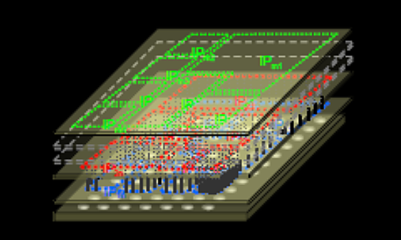
Supporting next-gen package development, up to 2.xD and 3D
Semiconductor Contract Processing
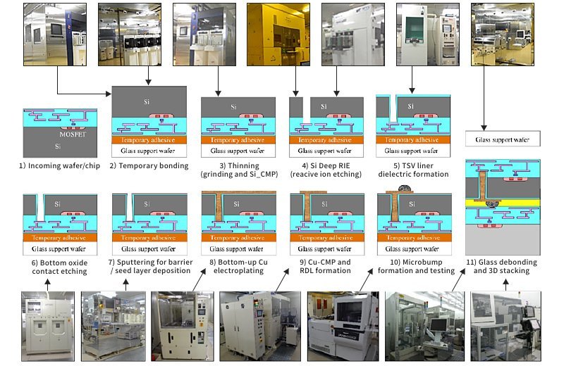
Seika assists customers with development and prototyping at one of the country's leading 12-inch production lines. The services we provide range from Test Element Group (TEG) fabrications to Si interposer, Through Silicon Vias (TSV) formation, deposition, RIE, microbump formation, and MEMS processing.
Applying 3D IC manufacturing technologies, we respond flexibly to processing needs of all kinds. Whether customers require small-lot or various processing, Seika provides one-stop service for single to complex processes using technology and equipment for TSV formation.
Contract processing services applying 3D and FOWLP technology make Seika a valuable ally for customers developing advanced packaging.
Highlights
- Integrated support from wafer thinning and TSV formation to rewiring, chip-to-chip bump formation, bonding, and gap filling
- R&D and prototyping support through 3D stacking of IC chips
- Prototyping and sample provision for 3D LSI devices using 2, 8, or 12-inch wafers
- Prototyping and small-volume production of silicon interposers using 12-inch wafers
- Fabrication of other structures using LSI and MEMS processes
Seika-Owned Equipment Used in All Production Processes
Examples of Contract Processing Inquiries
- Companies struggling to perform prototyping at their own facilities and considering outsourcing
- Companies who already outsource but have difficulty managing individual processes outsourced to several suppliers
- Companies requiring TEG wafer fabrication to develop basic 3D bonding technologies (hybrid or bump bonding)
- Companies developing 3D IC materials or equipment
Companies prototyping TEG wafers for testing or evaluation - Companies testing under various conditions
- Companies for whom minimum order quantities are a barrier that prevents progress toward goals
For product inquiries, please submit the contact form.
Related products
-
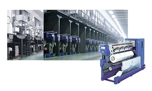
Textile and Film Equipment
Film Manufacturing Equipment -

Measuring Equipment
Online Gas and Liquid Analyzers (G800/L800) -

Power Generation Equipment
Wind Power -

Power Generation Equipment
Biomass Power -

Power Generation Equipment
Hydropower -
Power Generation Equipment
Solar Power -

Environment and Preservation Equipment
Power Generation Equipment
Natural Pellets -
Textile and Film Equipment
HYPOX Polymer Removal Systems -
Textile and Film Equipment
Synthetic Fiber Production Equipment -
Environment and Preservation Equipment
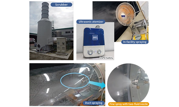
NOZEPAL Industrial Deodorizers -
Food and Pharmaceutical Equipment
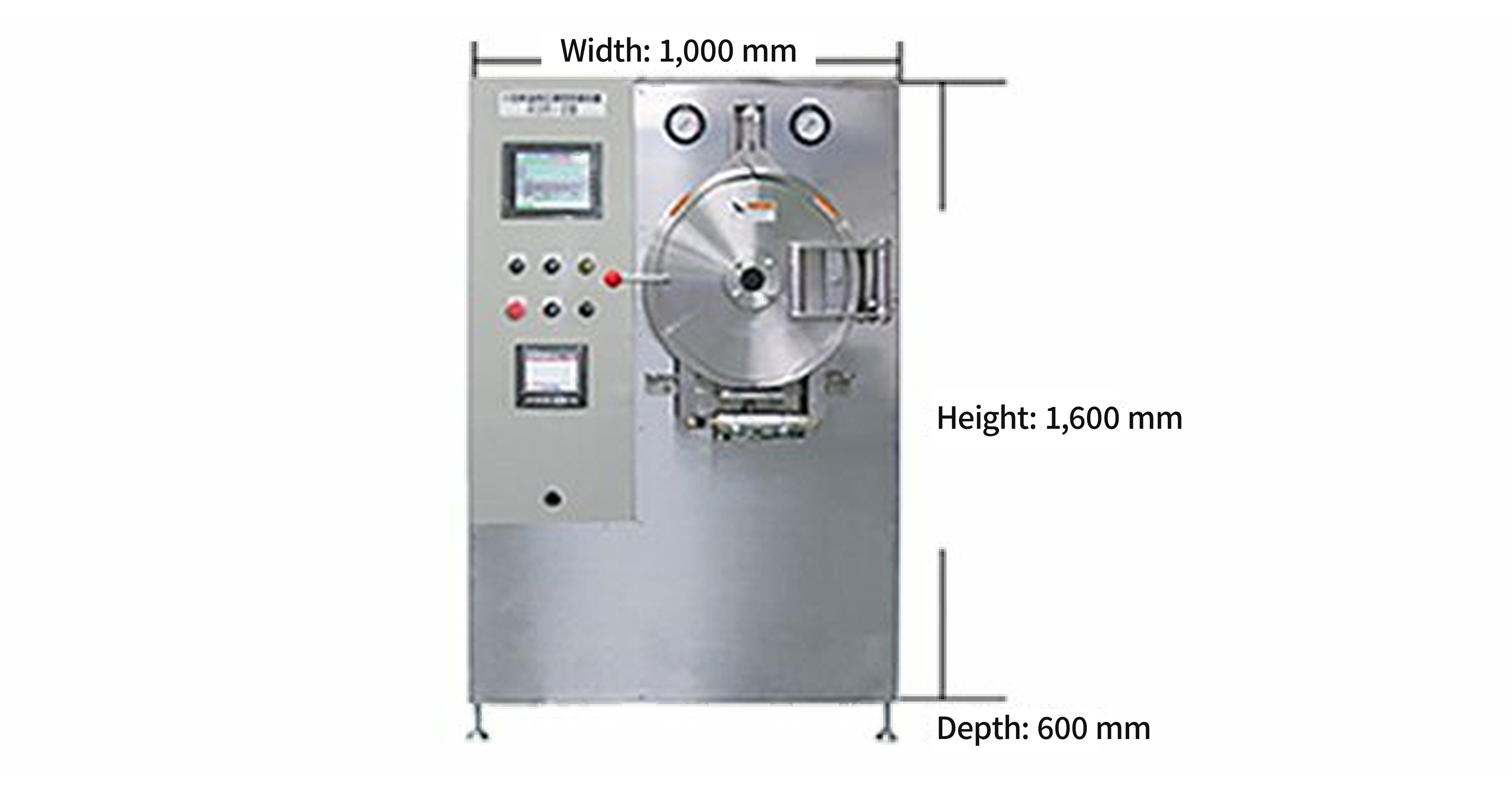
Compact, High-Temperature/Pressure Retort Sterilizers -
Textile and Film Equipment
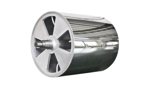
Large Industrial Rolls -
Food and Pharmaceutical Equipment
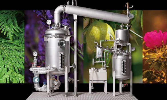
Essential Oil Decompression Steam Distillers -
Power Generation Equipment
General Industrial Machinery
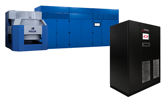
Battery-Free Flywheel UPS Systems -
Semiconductors, Electronics
Semiconductor Contract Processing -
Measuring Equipment
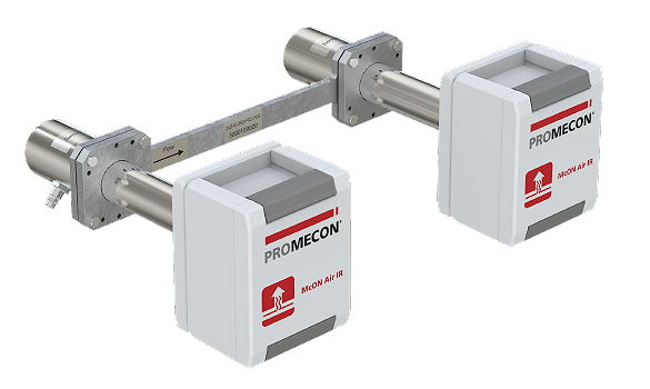
McON IR Sensors -
Measuring Equipment
Environment and Preservation Equipment
Handheld Gas Leak Inspection System -
Measuring Equipment
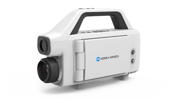
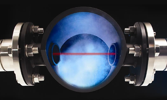
Laser Gas Analyzers -
Measuring Equipment
Food and Pharmaceutical Equipment
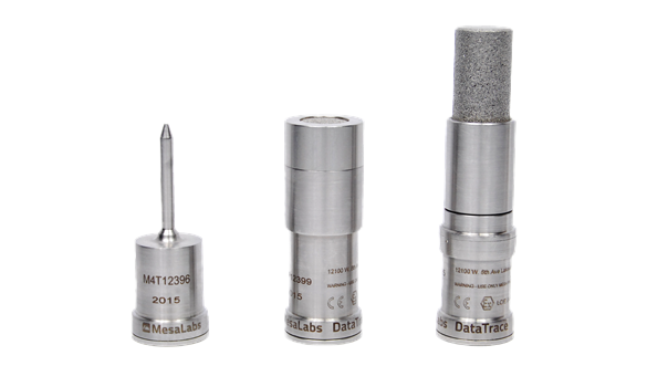
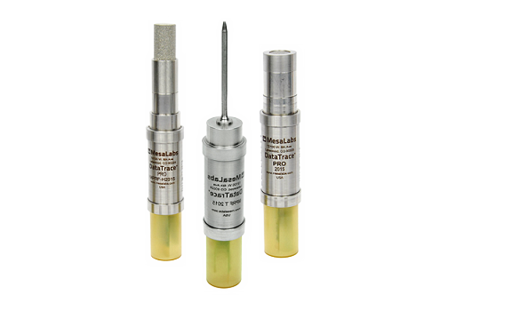
DataTrace Micropack III -
Measuring Equipment
Food and Pharmaceutical Equipment
DataTrace Micropack RF -
Environment and Preservation Equipment
Automation, Digital Transformation
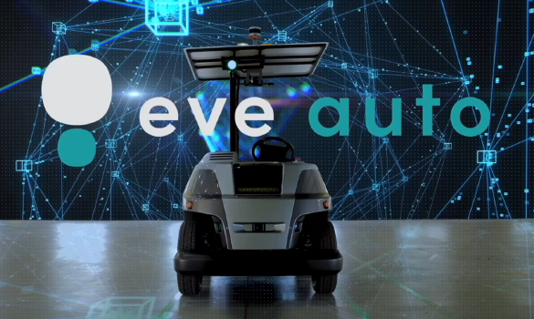
eve auto -
Measuring Equipment
Environment and Preservation Equipment
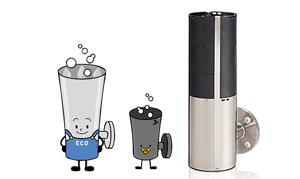
Seika Ecorator Diffuser Tubes -
Power Generation Equipment
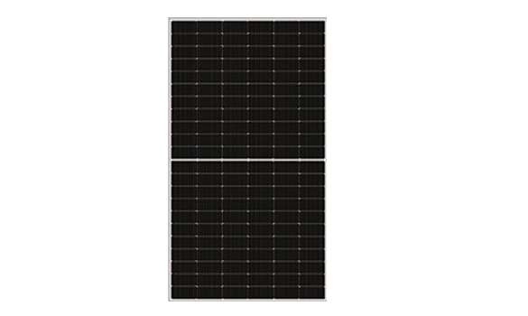
Ultralight Solar Panels -
Measuring Equipment
Automation, Digital Transformation
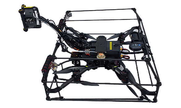
UT Drone-Based Plant Inspection